 Summary
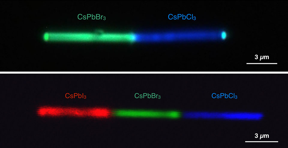
Halide perovskite nanostructures are created with two distinct regions of different compositions, forming heterojunctions. These structures utilize specific combinations of elements.
Applications
- Solar power generation
- Advanced LED lighting
- Sensitive light detection
Benefits
- Improved optoelectronic efficiency
- Tunable material properties
- Enhanced charge separation
- Broadened light absorption
Background
Perovskite materials are crucial for high-efficiency optoelectronic devices, including solar cells and LEDs, due to their excellent light-matter interaction. There is a significant need for advanced materials with tunable properties to enhance device performance. Existing methods often face challenges in precisely controlling electronic properties and charge carrier dynamics within nanoscale structures. Optimizing device efficiency requires overcoming limitations in material design and interface engineering for effective charge separation and transport.
Technology Description
Scientists at Berkeley Lab have developed a novel halide perovskite nanostructure incorporating heterojunctions. This nanostructure features two regions with distinct chemical compositions.
This technology forms precise heterojunctions within a single halide perovskite nanostructure by varying the halide components. This nanoscale compositional engineering allows for tailored electronic and optical properties, enabling advanced applications in areas like photovoltaics and optoelectronics that benefit from tunable bandgaps and efficient charge separation.
Development Stage
TRL 3: Proof of concept
Principal Investigator
IP Status
Patent pending
Additional Information
Dou, L. et al. (2017). Spatially resolved multicolor CsPbX 3 nanowireheterojunctions via anion exchange. PNAS, 114 (28) 7216-7221. https://doi.org/10.1073/pnas.1703860114
Opportunities
Available for licensing or collaborative research