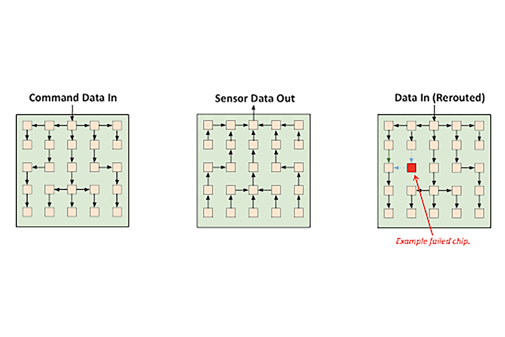
February 15, 2022, Berkeley, CA – Lawrence Berkeley National Laboratory (Berkeley Lab) scientists have developed a technique to automatically bypass failed Application Specific Integrated Circuits (ASICs) deployed in large arrays by rerouting dynamically around them. In the novel system, dubbed “Hydra I/O,” each ASIC chip is connected to its nearest neighbors on all four sides, unlike in traditional arrayed systems where chip-to-chip data paths are typically hardwired. This configuration allows data to be rerouted to adjacent neighbors upon the failure of an individual chip or multiple chips. The system includes software that dynamically reroutes commands or read-back data in these instances of chip failure in a way that is transparent to the user.
“To address the possibility of chip failure, current systems require building in significant redundancy in the event of chip failure,” said Carl Grace, leader for Berkeley Lab’s Integrated Circuits and Semiconductor Detectors Group. “The Hydra I/O system negates the need for expensive redundant systems, and it is highly resilient by design.”
The system was originally developed by Berkeley Lab for the Deep Underground Neutrino Experiment (DUNE) in which the custom chips that instrument the particle detectors will be placed in a sealed, cryogenic-liquid-filled cryostat located underground. Because the chips are physically inaccessible, the scientists developed a way to address inevitable chip failure during the experiment’s anticipated 30-year lifetime. The system was named “Hydra I/O” because when a single point fails, the rest of the system continues to function. This capability is similar to the way that the Internet automatically reroutes traffic around failed servers.

Fig. 2. Detector board showing 100 ASICs connected using a Hydra network.
Lab scientists Dan Dwyer and Grace, principal investigators for Hydra I/O, quickly recognized its potential applications in other environments where repair or replacement of ASIC arrays is similarly challenging or costly, such as in space, underwater, in remote locations, or in 5G systems that feature multiple phased arrays.
“The repair or replacement of failed ASICs chips is especially challenging where chips are inaccessible, as in the DUNE project,” said Dwyer, lead of Berkeley Lab’s Neutrino Physics group. “It was critical to the scientific mission that the tiles in the neutrino detectors are highly resilient. In our current prototype detector we have experienced roughly a dozen chip failures, and the Hydra I/O has made those failures non-events.”
The system is highly scalable. To date, the Berkeley Lab team has successfully operated a prototype detector system containing 1,600 ASICs coupled to almost 100,000 sensors. The Berkeley Lab team plans to build hundreds of thousands of ASICs for the DUNE project; further scaling the technology is very feasible.
For information on licensing this technology, contact ipo@lbl.gov.
Founded in 1931 on the belief that the biggest scientific challenges are best addressed by teams, Lawrence Berkeley National Laboratory and its scientists have been recognized with 13 Nobel Prizes. Today, Berkeley Lab researchers develop sustainable energy and environmental solutions, create useful new materials, advance the frontiers of computing, and probe the mysteries of life, matter, and the universe. Scientists from around the world rely on the Lab’s facilities for their own discovery science. Berkeley Lab is a multiprogram national laboratory, managed by the University of California for the U.S. Department of Energy’s Office of Science.
DOE’s Office of Science is the single largest supporter of basic research in the physical sciences in the United States, and is working to address some of the most pressing challenges of our time. For more information, please visit science.energy.gov.
