APPLICATIONS OF TECHNOLOGY:
- Transmission Electron Microscopy (TEM)
- Microelectronics
- Microelectromechanical systems (MEMS)
- Electron and photon-based characterization techniques
BENEFITS:
This new fabrication method for ultra-thin membranes holds several important advantages over the current state-of-the-art. These membranes are:
- Highly customizable
- Electrically conductive
- Scalably-produced
- Mechanically robust
- Compatible with subsequent lithography steps (can be integrated into larger microelectronic circuits or devices)
BACKGROUND:
Generally, there has been very little innovation in the materials available as ultra-thin (i.e. several nanometers) suspended membranes. The fabrication of such membranes typically requires growth of the membrane material(s) on a substrate, and then removal of the supporting material(s) under it to yield a free-standing film. However, there are well-known fabrication difficulties involved in releasing such thin membranes without damage. Furthermore, the membrane materials available via scalable production methods are highly limited. Atomic layer deposition (ALD) allows for the growth of a wide variety of ceramic materials, including electrically conductive ceramics, that are highly uniform and pinhole free at ultra-low thicknesses.
TECHNOLOGY OVERVIEW:
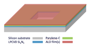
Berkeley Lab scientists have developed a new fabrication method for making ultra-thin suspended membranes of a variety of materials. These free-standing membranes can be as thin as several nanometers, and are fabricated using atomic layer deposition (ALD) and a sacrificial polymer that allows for the release of ultra-thin ceramic films without damage.
The membrane material and thickness are highly customizable, and two or more ALD materials can be combined or alternated based on the needs of the application. For example, materials can be selected to provide application-specific chemical resistance, conductivity, or surface functionalization, while still maintaining electron transparency and mechanical robustness. The fabrication process involved in this invention results in an ultra-thin, robust, and customizable membrane that can be fabricated using standard and scalable methods. There are many potential uses for a conductive membrane that is only several nanometers thick. Beyond use as electron-transparent windows, membranes are often used in microelectronics as sensors or diaphragms.
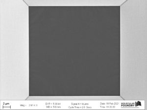
With this new fabrication method, the first device created by Berkeley Lab scientists is an electrically conductive and electron-transparent window suited for both conventional and liquid cell Transmission Electron Microscopy (TEM). The window comprises titanium nitride (TiN) and has advantages over the current state-of-the-art (silicon nitride, graphene, or amorphous carbon), as it is the first electrically conductive TEM window fabricated using scalable methods.
DEVELOPMENT STAGE: Proven principle
RELATED TECHNOLOGY:
Ultrathin Free-standing Oxide Membranes for Electron and Photon Spectroscopy 2020-094
Low Cost Fabrication of Thin-Film Ceramic Membranes for Nonshrinking Substrates IB-1304
INVENTORS:
STATUS: US Patent Pending US20220306460A1
OPPORTUNITIES: Available for licensing or collaborative research.

