The three new technologies described below, developed by Alex Zettl and his team from Berkeley Lab’s Materials Sciences Division, add to Berkeley Lab’s robust patent portfolio of nanodevices. These new inventions offer opportunites for quantum advancements in wireless communication, MEMS capababilities, and mass sensing, among other applications. All of the inventions have patents pending and are available for licensing or collaborative research opportunities.
Forceful MEMS/NEMS Nanoactuator (IB-2008a)
Nanoresonator for Precise Position and Mass Sensing (JIB-2124)
Voltage-Controlled, Autotransducing Microwave Oscillator (IB-2008b)
BERKELEY LAB’S POWERFUL NANOACTUATOR

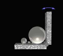
Metal atoms are transported via electric current from the large metal droplet on the right to the small one on the left. The droplet on the left grows until it touches the shrinking droplet on the right. Surface tension then causes the larger droplet to absorb the smaller one in a relaxation event, which applies great force to push the lever to the right.
Forceful MEMS/NEMS Nanoactuator
IB-2008a
APPLICATIONS OF TECHNOLOGY:
- Nanoscale drive mechanisms for integrated MEMS/NEMS, e.g. motors, electromechanical switches, drives for mirrors in projectors and routers, microfluidic control valves
ADVANTAGES:
- Scalable and simple to construct
- Several orders of magnitude more powerful per unit volume than conventional drives
- Compatible with existing semiconductor architectures, manufacturing processes, and operating conditions
- Extremely rapid, wear-free mechanical response
- Uses dc voltage as low as 1v
DESCRIPTION:
Alex Zettl and colleagues have invented the first device to harness the incredible force of surface tension at the nanoscale, which can become the dominant force for systems this small. The Berkeley Lab nanoelectromechanical actuator offers several features that will enhance switching and motor functions for MEMS devices: it’s nanoscale yet simple to construct and manufacture in bulk; it’s extremely powerful with a mechanical frequency range from dc to gigahertz; the action is frictionless and driven by extremely low voltage. The new actuator can also be integrated into existing semiconductor architectures and manufacturing processes and functions at semiconductor operating temperatures.
In the Berkeley Lab invention, a molten metal droplet governed by dc current grows and shrinks on a nanotube substrate like a miniature hydraulic press, applying force to a lever, mirror or other object. The mechanism is reversible and its speed can be controlled by increasing or reducing the voltage.
STATUS: Issued U. S. Patent #7515010. Available for licensing or collaborative research.
REFERENCE NUMBER: IB-2008a
Tunable Carbon Nanotube Resonator
JIB-2124
APPLICATIONS OF TECHNOLOGY:
- Telecommunications and radio frequency signal processing
- cell phone electronics and antennas
- radio frequency filters
- Attogram mass detection
- lab on a chip
- artificial nose
- pathogen detection
- Attonewton force detection
- Sub-nanometer distance measurement
- nanotube electromechanical system (NEMS) strain gauge
- STM/AFM piezo position feedback
ADVANTAGES:
- Wide frequency range as compared with silicon and other tunable resonators
- Simpler physical model, atomically perfect structure
- Low density
- High Young’s modulus
- Tunable, telescoping facility replaces current resonators of many different lengths
- Label-free chemical species detection
DESCRIPTION:
Alex Zettl and his team at Lawrence Berkeley National Laboratory have developed a high-Q, tunable, megahertz-to-gigahertz range mechanical resonator composed of a telescoping multiwall carbon nanotube (MWNT) clamped at both ends. The invention depends on methods for preparing ultra-high quality multiwall carbon nanotubes whose core can be telescoped out.
The resonator is created by peeling off the outer shells at the tip of a nanotube and attaching strong, durable contacts at both ends. A mobile, piezoelectrically controlled contact is extended or retracted to tune frequency of the resonator, by telescoping a nanotube core in or out of the outer nanotube shells.
Current resonators rely on tensioning a nanotube, but being able to control the length rather than tensioning, by developing contacts between the nanotube and a metal electrode, offers numerous advantages. These contacts can overcome the natural attractive molecular (van der Waals) forces and do not degrade with nanotube vibrations.
Given their superior properties, the resonators and should find immediate application in microelectromechanical or nanoelectromechanical systems (MEMS/NEMS) devices. Many potential applications can be envisaged in precise mass, force, position, and frequency measurement. In addition, detection of resonant energy transfer between a properly tuned nanoresonator and a target molecule could make possible label-free chemical detection of any molecular species by a single device, far more efficiently than current sensing devices, which are limited to identifying individual molecular species.
STATUS: Issued U. S. Patent #7,915,973. Available for licensing or collaborative research.
FOR MORE INFORMATION:
Jensen, K., Girit, C., Mickelson, W., Zettl, A.,”Tunable Nanoresonator.” In Electronic Properties of Novel Nanostructures, AIP Conference Proceedings, 2005, 786: 607-610.
REFERENCE NUMBER: JIB-2124
Voltage-Controlled, Autotransducing Microwave Oscillator
IB-2008b
APPLICATIONS OF TECHNOLOGY:
- High frequency oscillation for enhanced signal processing for wireless communication, e.g. RF signal filtering
ADVANTAGES:
- Tunable with a frequency range from dc to GHz
- Provides electrical/mechanical transduction
- Wear-free, scalable, and simple to construct
- Compatible with existing semiconductor architectures, manufacturing processes, and operating conditions
- Simple dc voltage input yields ac current response
DESCRIPTION:
Alex Zettl and colleagues at Berkeley Lab have adapted a controlled droplet pulsation action to provide tunable, high frequency nanoscale oscillation. The invention could form the basis for an advanced generation of wireless RF/microwave communication devices, offering a frequency range that could expand wireless channels, low voltage operation, nanoscale dimensions, and a mechanism that naturally yields mechanical-to-electrical transduction. The device converts electrical dc input to ac mechanical oscillation and automatically converts that oscillation to electrical ac output. The oscillator can be integrated into semiconductor manufacturing processes and functions at semiconductor operating temperatures.
STATUS: Issued U. S. Patent #7515010. Available for licensing or collaborative research.
FOR MORE INFORMATION:
REFERENCE NUMBER: IB-2008b
SEE THESE OTHER BERKELEY LAB TECHNOLOGIES IN THIS FIELD:
- Controllable, Reversible, Nanoscale Mass Conveyor
- Directed-Assembly of Carbon Nanotubes (CNTs)
- Powerful Linear Nanomotor
- Scalable Methods for Growing, Shaping, and Placing Nanostructures