APPLICATIONS OF TECHNOLOGY:
- In vitro diagnostics
- Biopharmaceutical R&D
- Systems biology laboratory research
- Single-cell “omics”
- Lab-on-a-chip analyses
- Food safety testing
- Environmental monitoring
ADVANTAGES:
- Robust and scalable silicon fabrication technologies
- High-throughput multiplexing, i.e., processing multiple analytes sequentially
- High-sensitivity
- Eliminates potential sample carryover
- Can be re-used
- Improved reproducibility for parallel analysis
- Multi-nozzle design mitigates salt and debris clogging
- Integrated designs for lab-on-a-chip
ABSTRACT:
A team of Berkeley lab researchers led by Peidong Yang and Daojing Wang has developed a novel silicon-based microfluidic system that can sequentially spray up to 96 different nanoscale analyte samples into the ion cone of an electrospray ionization mass spectrometer (ESI-MS). This readily scalable technology enables serial interrogation of multiple analytes from a sequence of samples, providing a clear path to an automated lab-on-a-chip for single cell analysis, which has been described as the new frontier of omics research.
The technology builds upon earlier work by the Berkeley Lab team that produced an electrospray emitter tip featuring 10 microscale nozzles fed by a single channel, akin to a showerhead. In that technology, IB-2211, fluid is sent to the tip where the 10 nozzles each emit an ionized mist of nanoscale droplets propelled by an electric charge.
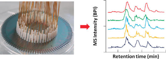
The new Berkeley Lab technology, called a monolithic multinozzle emitter array (MEA) chip, lays out 96 of the 10-nozzle emitter tips around the circumference of a 3-inch silicon wafer, giving it the appearance of a radial saw blade (see figure). With its edge placed horizontally at the inlet of a mass spectrometer, the array can be rotated to place each tip briefly, in sequence, in front of the ion cone, at which time the multinozzle tip will emit its ionized droplets for analysis. Each multinozzle tip is fed by its own microfluidic channel coming from the center of the wafer, where a circle of 96 separate capillary tubes delivers a liquid sample to each channel.
Among the critical features of this innovative design are sharpened multinozzle tips. The sharp edges maintain, throughout the array, an electric field high enough to overcome charge-charge interactions that would otherwise become problematic as the number of nozzles increases. The silicon wafer architecture is readily scalable; for example; a 6-inch wafer could have 384 nozzles. The MEA’s multinozzle design is suitable for automated mass spectrometry equipment and can provide the integration, high-throughput, and high-sensitivity required for clinical diagnoses and single-cell analyses.
Mass spectrometry is a powerful tool in the burgeoning field of omics, the large-scale study of genes, transcripts, proteins, metabolites, lipids, and their interactions. Future expansion of the field requires development of advanced tools, such as the Berkeley Lab MEA, to automate and integrate such analyses.

The 96-emitter array chip (L) and a graph (R) demonstrating the reproducibility of MEA emitters with mass spectrometry detection for randomly selected MEA emitters from the 96 emitters on the MEA chip.
DEVELOPMENT STAGE: Bench scale prototype.
STATUS: Issued U. S. Patent #9,793,477. Licensed in some fields of use. Contact ipo@lbl.gov to discuss remaining fields of use.
FOR MORE INFORMATION:
SEE THESE OTHER BERKELEY LAB TECHNOLOGIES IN THIS FIELD:
Electrospray Emitters for Integrating Mass Spectrometry with Microfluidic Devices, IB-2211
REFERENCE NUMBER: IB-2977