Berkeley Lab researchers have developed two approaches for increasing the charge efficiencies of electrodes used to produce flexible organic light emitting diodes (OLEDs) and solar cells. Both approaches will reduce manufacturing and packaging costs. These technologies have patents pending and are available for licensing or collaborative research.
Solvent Processed Nanotube Composites
IB-2044

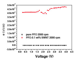
Conductivity of pure PFO polymer (black) and PFO/SWNT composite film (red). See publication link below for more information.
APPLICATIONS :
Composites for transparent electrodes and/or light emitting layers used in
- OLED displays for consumer electronics, digital video, and medical imaging devices, or built into architectural and automobile windows and flexible plastics
- Organic photovoltaics
- OLEDs for lighting
ADVANTAGES:
- Solvent processed, ink jet printable
- More efficient charge injection and higher conductivity than conventional conducting polymers
- Transparent (= ITO film)
- Reduced drive voltage
- Compatible with flexible substrates
- Longer material lifetimes than devices made with active metal
DESCRIPTION:
A new class of conductive polymers developed at Berkeley Lab uniformly suspends and disperses carbon nanotubes, enabling them to function efficiently as charge injectors in the electrodes and light emitting layers of OLEDs and organic solar cells. Currently, OLEDs cathodes are thermal vacuum evaporated due to the use of reactive metals for electron injection. The use of calcium or lithium also requires air-impenetrable packaging. In contrast, devices made using Berkeley Lab’s air-stable cathode materials can be solvent processed and applied using ink jet printing or spin coating. They also have relaxed packaging requirements.
Unlike most OLEDs that incorporate metals in the cathode, the Berkeley Lab OLEDs are transparent. Transparent OLEDs can be used to display video, images, and other information in applications where the user still can see through the substrate, such as with windshields and windows. While ITO films are also transparent, they are brittle and require plasma deposition. The Berkeley Lab materials are flexible and promise to be low-cost – making inexpensive, roll-up, digital display technology a near-future possibility.
Gao Liu, John Kerr and colleagues have demonstrated initial efficiencies of three percent for OLED devices incorporating the poly(di(oxytrioxadecane)fluorine)(PFO)/nanotube composites, with a clear research path towards significant increases. The nanotubes have remained suspended in the PFO for over four months, far exceeding the six day limit achieved in other nanotube/polymer systems. The suspension is sustainable because the polymer is amphiphilic and wraps its polar side chains around the nanotube. Both the backbone and side chains of the polymer can be adapted to accommodate various applications.
STATUS: Published Patent Application. Availble for licensing or collaborative research.
FOR MORE INFORMATION:
Zhang, T., Simens, A., Minor, A., Liu, G., “Carbon Nanotube-Conductive Polymer Composite Electrode for Transparent Polymer Light Emitting Device Application,” PMSE 2006.
OLEDs with Air-stable Structured Electrodes
IB-2231
APPLICATIONS :
- Displays for consumer electronics, digital video and medical imaging devices
- Displays for architectural and automobile windows and flexible plastics
- OLEDs for lighting
ADVANTAGES:
- Significantly improved OLED performance at reduced drive voltages due to
- enhanced charge injection efficiency and
- more balanced charge distribution
- Increased OLED device lifetime
- Capable of scale-up manufacturing–either “top-down” or “bottom-up” processing
- Enables the use of flexible substrates
DESCRIPTION:
Scientists at Berkeley Lab have modified the cathode-organic layer of an OLED device to significantly enhance electron injection efficiency and reduce the sensitivity of the cathode to environmental degradation by water and oxygen. Two approaches are used:
An ordered arrangement of nanostructures (top-down processing) or
A nanomaterial interfacial layer (bottom-up processing).
This technology represents a significant improvement over existing technology. Currently, the interface between an OLED device’s cathode and organic layer is a resistant barrier that inhibits the efficient flow of electrons. This barrier can also create heating that damages the OLED. Additionally, low work function metals used to reduce operating voltage and improve device yield are physically and chemically unstable and difficult to fabricate into a thin layer.
The Air-stable Nanostructured Electrodes promise to significantly reduce the drive voltage necessary to induce light emission inside organic materials and will thereby increase the energy conversion efficiency of the OLEDs. The ordered arrangements of nanostructures or nanomaterials to enhance charge injection efficiently overcome the large energy barrier at the cathode-organic layer interface. Charge balance between holes and electrons is improved, a steeper rise in current as a function of voltage is realized, and electrical-optical conversion efficiency is increased.
Using less reactive materials makes the cathode more resistant to degradation than conventional metal electrodes. This feature increases OLED device lifetime, simplifies packaging requirements and makes it amenable to scale-up manufacturing processes.
STATUS: Published Patent Application. Available for licensing or collaborative research.
FOR MORE INFORMATION: