APPLICATIONS OF TECHNOLOGY:
- Photovoltaics
- LEDs
- Transistors
- Diodes
- Optical color conversion
- Oriented or ordered nanocrystals
- Memory devices
- Quantum information processing
- Artificial photosynthesis
- Mechanical reinforcement
- Catalysis
ADVANTAGES:
- Enables fabrication of complex nanocrystal geometries
- Each component of the nanocrystal can be independently tuned by varying composition, length, diameter, and crystal phase
- Increases possible points of contact between a nanocrystal and a substrate
- Increases possible number of connections to electrical leads
ABSTRACT:
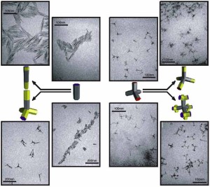
Berkeley Lab researchers have demonstrated a general approach for fabricating inorganically coupled quantum rods and dots by connecting them epitaxially at branched and linear junctions within single colloidal nanocrystals. The researchers have created branched semiconducting nanorods, nanotetrapods, and other complex geometries where the branching location, branch lengths, and diameters can be controlled and the composition of each rod section may vary. Using the Berkeley Lab method, branching points can be introduced not only at nucleation but also later in the growth process.
The inorganic materials that can be used in this technique have optical, mechanical, electrical, magnetic, catalytic, and other functional properties that can now be controllably combined in a single geometrically complex nanocrystal. This capability invites investigation into new fields such as quantum information processing and artificial photosynthesis and promises improvements to solar cells, LEDs, and transistors.
STATUS:
- Patent Pending. Available for licensing and collaborative research
REFERENCE NUMBER: IB-1948
