APPLICATIONS OF TECHNOLOGY: Windshields and windows Solar panels Lenses for cameras, endoscopes, laparoscopes, and other optical devices Eyewear – goggles and glasses Dental mirrors ADVANTAGES: Stable over time Inexpensive Does not require UV-light activation Excellent optical properties (high transmittance; low reflectance and refractive … [Read more...] about Superhydrophilic Nanostructure for Antifogging Glass IB-2687
Atomically Flat Crystal Surfaces IB-2549
APPLICATIONS OF TECHNOLOGY: Semiconductor fabrication and processing High density magnetic recording devices Crystal preparation Materials science research ADVANTAGES: Simple, self-assembling Doesn’t require lithographic pre-patterning of the surface Low cost Can be used for wide range of materials ABSTRACT: Devices once fabricated at … [Read more...] about Atomically Flat Crystal Surfaces IB-2549
Modifying Nanocrystal Surfaces for Molecular Imaging and Electrical Devices IB-2616
APPLICATIONS OF TECHNOLOGY: Fluorescent labeling Biological sensing - Forster Resonance Energy Transfer (FRET) Electrical devices (sensors, LEDs, photovoltaics) Catalysis Fillers in composite materials ADVANTAGES: Smaller probe enables improved mobility within the cell Can be used to enhance insulation or conduction in electronic devices Any … [Read more...] about Modifying Nanocrystal Surfaces for Molecular Imaging and Electrical Devices IB-2616
Biomimetic Peptoid Polymer 2D Nanosheets IB-2633
APPLICATIONS OF TECHNOLOGY: Medical: Bioanalysis Biosensors Surface display of biomolecules on chemically defined surfaces Catalytic reactive membranes for filtration and separation Electronic: Sensors Batteries Fuel cells Capacitors ADVANTAGES: Unexpectedly high biological and thermal stability Resists degradation … [Read more...] about Biomimetic Peptoid Polymer 2D Nanosheets IB-2633
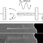
Nanotube Radio for Communications and Medical Applications IB-2431, 2432
APPLICATIONS OF TECHNOLOGY: All-in-one radio receiver for cell phones/wireless networks/GPS and other electronic devices Radio controlled devices that can exist inside the body, e.g. used as drug release triggers, diagnostic instrumentation, interfacing with muscle or brain function Ultra small hearing aid RF antenna, tunable pass filter, amplifier, or … [Read more...] about Nanotube Radio for Communications and Medical Applications IB-2431, 2432


