APPLICATIONS OF TECHNOLOGY:
SIZE REDUCTION LITHOGRAPHY PROCESS
- Ultra-sensitive biological and chemical sensing
- Microchips
- Catalysis
- Nanocomputing and nanoelectronics
ADVANTAGES:
- Uses standard semiconductor fabrication equipment and techniques to produce nanosize semiconductors on a wafer scale
- Produces smaller feature sizes and is much less time consuming than scanning probe lithography-based techniques, e.g. electron beam lithography
- Unlike chemical vapor deposition (CVD) methods to grow nanostructures, this process provides uniform dimensions and doping levels, and precise control over the position of the nanosensors
- Generates far smaller patterns than are possible with optical lithography
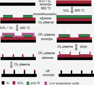
ABSTRACT: Researchers at Berkeley Lab have succeeded in fabricating nanowire arrays with feature dimensions of 10 nm or less on a wafer-sized scale. The method employs standard semiconductor manufacturing techniques to achieve highly uniform dimensions and doping levels as well as precise control over the location of the nanosensors.
Yang-Kyu Choi, Ji Zhu, Jeff Grunes, Jeffrey Bokor, and Gabor Somorjai first fabricated 600 nm polysilicon patterns and then combined conformal deposition and anisotropic etching processes to produce 20 nm single crystal silicon nanowire arrays. Further oxidation of the nanowires and etching in hydrogen fluoride further reduced feature sizes to sub 10 nm. Silicon nanowire structures fabricated by this method can be used as masks for producing high surface area devices using nanoimprint lithography. The imprinted wafers can be doped via ion implantation and electrical contacts formed using standard lithography.
In research to date, the Berkeley Lab scientists have chosen to produce 7×10⁸ nanowires on a 4 inch silicon substrate to obtain a total patterned surface area of ~ 1cm2 in a matter of days. If this was done with electron beam lithography, it would take years and costs millions of dollars to produce as many sub-10 nm nanowires.
One important advantage of the Berkeley Lab fabrication method is that the feature size is determined by the thickness of the deposited material and not by the photolithography, which is typically the size-limiting factor. The invention is also faster and produces smaller feature sizes than electron beam lithography, which has the problem of scattering secondary electrons after the initial bombardment. Currently employed CVD methods are poorly controlled and slow, while the Berkeley Lab technique produces uniform dimensions and doping levels, and provides excellent control over the position of the sensors.
STATUS:
- Patent pending; available for licensing or collaborative research
FOR MORE INFORMATION:
REFERENCE NUMBER: IB-1997
